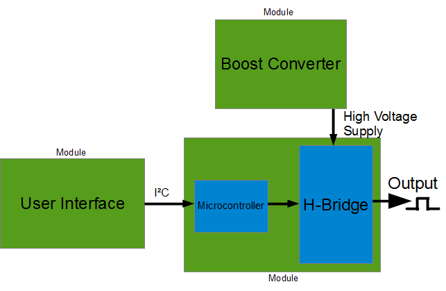
Block diagram
Block diagram
The design and construction of a programmable, modular, multi-channel high-voltage DC to AC inverter will be explained in the following report. These requirements for the system were established:
a peak to peak voltage of \(400~\textrm{V}\),
an output frequency of at least \(20~\textrm{kHz}\),
a modular and extensible system,
at least four output channels,
and a way to easily change the output frequency and amplitude via either a PC or the included user interface.
The chosen architecture consists of three types of modules, where only one will be needed multiple times. The boost converter module generates the necessary high-voltage and can be replaced with an off-the-shelf lab power supply. The user interface module connects to the H-bridge modules via an I²C bus and to the PC via USB. It includes a display and buttons to change the parameters without a computer.
The H-bridge module is the core of the system. Multiple output channels can be implemented in a single module. The input high-voltage supply is regulated to the desired amplitude and then switched with an H-bridge. The generated square wave is accessible through a connector. A micro-controller generates the control signals for the H-bridge and communicates with the user interface module. The desired output frequency is generated by this micro-controller.
The MAX1771 is a fully integrated Boost Converter Controller IC with an integrated gate driver. A maximum switching frequency of \(300~\textrm{kHz}\) enables the use of relatively small inductors even for high output voltages. The circuit can be configured to work in a bootstrapped or non-bootstrapped mode. An input range of \(2~\textrm{V}-16.5~\textrm{V}\) enables the use of high-power MOSFETs in non-bootstrapped mode (as \(V_{GS(th)}\geq10~\textrm{V}\) for most devices).
The output voltage can be adjusted via two resistors or is fixed at \(\text{12~\textrm{V}}\). The MAX1771 is available in the SO8 and DIP8 package and therefore well suited for prototyping.
The following specifications were chosen: \(V_{F}=1~\textrm{V}\), \(V_{out}=220~\textrm{V}\), \(V_{in}=12~\textrm{V}\), \(V_{sat}\approx1~\textrm{V}\) and \(I_{out(max)}=150~\textrm{mA}\).
Using the following equations, the values for the inductor \(L\), the maximum current flowing through the inductor, FET and diode \(I_{switch(peak)}\) were calculated.
\[t_{on}/t_{off}=\frac{V_{out}+V_{F}-V_{in}}{V_{in}-V_{sat}}=19\]
\[I_{switch(peak)}=2I_{out(max)}(t_{on}/t_{off}+1)=6~\textrm{A}\] \[L\geq\frac{V_{in}\cdot2~\mu\textrm{s}}{I_{LIM}}=4~\mu\textrm{H}\]
In the next step a matching MOSFET was chosen. The IRF740 was selected for its low price and easy availability. It has a \(V_{DS(max)}=400~\textrm{V}\) and is therefore suited for this application. The typical total gate charge for this device is given as \(Q_{g,TOT}=41~\textrm{nC}\). This is small enough to be driven from the EXT pin of the MAX1771 but will require a larger bypass cap:
\[C_{bypass}\geq\frac{Q_{g}}{200~\textrm{mV}}=205~\textrm{nF}\]
The integrated current-limit feature of the MAX1771 requires a shunt resistor between the MOSFET drain and ground. The required value was calculated as follows:
\[R_{sense}=\frac{85~\textrm{mV}}{I_{LIM}}=\frac{85~\textrm{mV}}{6~\textrm{A}}=14~\textrm{m}\Omega\]
The maximum dissipated power in the sense resistor has to be calculated to select an appropriate package:
\[P_{Rsense}=R_{sense}I_{LIM}^{2}=0.504~\textrm{W}\]
The components used have to be specified with the high output voltage in mind. The necessary voltage rating for each component on the output side of the circuit will be explained following the schematic from left to right, with the part designator given in brackets.
The IRF740 (Q1) is rated at \(V_{DS,max}=400~\textrm{V}\) which gives more than enough headroom.
The MUR440 rectifier diode (D1) is also rated at a working repetitive peak reverse voltage of \(400~\textrm{V}\).
Through-hole resistors (R2, R11, R4) and trimmer potentiometers (R12) are usually rated for voltages of at least \(200~\textrm{V}\), so generic components can be used.
To filter the ripple caused by the switching regulator high-quality capacitors are needed (C10 ... C14). Their voltage rating should exceed \(250~\textrm{V}\). Low-ESR types are preferable.
The LED at the output has two purposes: it indicates the presence of a high voltage and drains the output capacitors, thus increasing the safety of the device.
Components on the input side of the circuit are either less critical or were already specified.
The user interface is the least complex part of the system. It is based on an Arduino UNO, which is an inexpensive and widely used micro-controller development platform. It comes with USB and I²C support built-in and is supported by a vast selection of software libraries and example code. It was chosen to shorten the development-cycle of the user interface firmware.
The Arduino system can be extended by add-on PCBs called shields. For this system a custom shield with the necessary display, buttons and connectors was developed. The choice of parts was mainly determined by their availability. So a graphical display from the DOG series by Electronic Assembly and an ALPS rotary encoder were chosen. Two generic switches, an LED, several connectors and some support circuitry completed the shield.
The H-bridge board is separated in two parts: the micro-controller circuit and the high-voltage switches and regulation. These parts are not isolated from each other as they share the same ground. Both circuits will be explained in detail in the following.
The micro-controller circuit is based on the ATtiny861A from Atmel. This controller comes with I²C slave support and extensive timer features. The timers are used to generate the signals controlling the H-bridge. Two major features of the ATtinyX61A series make it especially suited for this application: the prescaler for Timer/Counter1 has 16 settings and the module integrates an independent dead time generator for each PWM channel. Using these features, the frequency linearity of the generated control signals is better than \(1\%\).
The power for the ATtiny861A is provided by an MIC5205-5.0, which is a linear regulator with fixed \(5.0~\textrm{V}\) output in a tiny package. Furthermore a DIL switch, two status LEDs and the communication connector surround the micro-controller. The DIL switch is used to select the I²C slave address the controller listens to. This allows several otherwise identical modules to be configured independently.
To synchronize several modules, a master clock can be distributed via the communication connector. It is buffered locally by a single inverter gate. Together with the interrupt line present on the connector a programmable phase-shift between multiple PCBs can be implemented.
The signals controlling the H-bridge are also brought out on the connector, however this feature is not used anymore.
This part of the circuit does the actual high-voltage switching. To be able to generate signals of different amplitudes, the incoming high-voltage supply of about \(210~\textrm{V}\) is regulated before entering the switching transistors. Each of the two present output channels comes with a linear regulator able to output voltages in the range of \(13.2-200~\textrm{V}\). For ease of implementation the LR8 high-voltage linear regulator from Supertex was chosen. It can withstand input voltages of up to \(450~\textrm{V}\) and output voltages in the range of \(13.2-440~\textrm{V}\). It also comes with integrated current and junction temperature limiting, which prevents circuit failure under over-load conditions. As this regulator uses a resistor network for feedback, the output voltage has to be dialed in via a ten-turn potentiometer.
Only low voltages and currents are present on the micro-controller side of the circuit, therefore generic components can be used. This is not true for the H-bridge and voltage regulator circuit: because of high voltages special care has to be taken in specifying the components.
To begin with, the specifications of critical parts in one half-bridge will be explained. The part designator is again given in brackets.
The gate resistors (R10, R11) have to be rated for the maximum current flowing when switching occurs. They have to be rated for \(330~\textrm{mW}\).
The switching transistors (FET7, FET8) were chosen for their fast switching time. Of course they have to withstand a drain-source voltage of at least \(250~\textrm{V}\).
As the IR2110 uses a bootstrap circuit to switch the upper n-FET the supporting parts (D4, C23) had to be specified according to the data-sheet. The diode has to have a peak reverse of at least \(V_{HV}+V_{DD}=200~\textrm{V}+12~\textrm{V}=212~\textrm{V}\). The ES2G is specified for \(V_{RRM}=400~\textrm{V}\) and should therefore work without a problem.
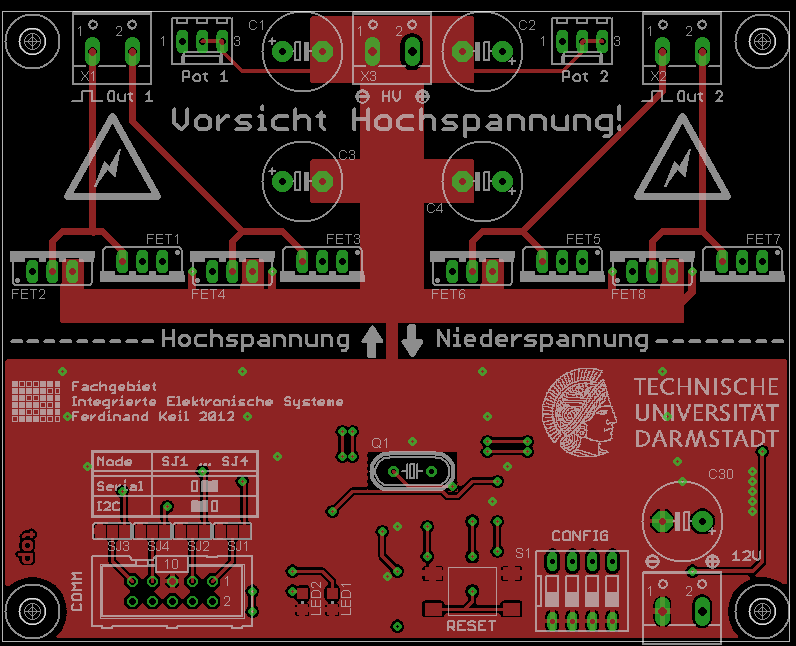
PCB layout - top
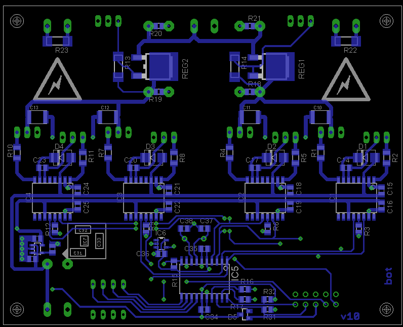
PCB layout - bottom
Critical parts of the PCB layout will be explained in the following section.
The circuit is divided in two parts: the low-voltage part in the lower half and the high-voltage part above it. Both share the same ground, but are connected by a small trace only. This is done to prevent high-frequency switching noise from propagating across the whole circuit. The high-voltage circuit part is not flood-filled with a copper pour to direct the ground currents in certain paths.
The high-voltage switching circuitry is grouped together as close as possible to minimize track inductance and shorten current loops.
All surface-mount components are placed on the bottom side of the PCB (with the exception of the LEDs and the reset switch). This prevents users from accidentally touching parts carrying high voltage, as leaded parts can easily be isolated, e.g. using shrink tubing.
The firmware for the micro-controllers on the H-bridge board and user-interface board was developed separately by two students. The controllers communicate over the I²C bus, where the user-interface board acts as the master and each H-bridge board as a slave node.
The micro-controller on the H-bridge board is mainly concerned with generating the requested waveforms. Therefor the advanced features of the integrated hardware timer are used. To support communication via IC the integrated two-wire hardware module is used.
The firmware for this board was written by Ferdinand Keil.
The user-interface board is based on the Arduino development platform. This eases the re-usability of available code and accelerates the development cycle. It also comes with USB support, which is used by the firmware to connect to LabView on a PC. The board can get its commands either via USB from a host PC or directly via the on-board display and encoder. The settings are forwarded over I²C to the slave nodes.
The firmware for this board was written by Manuel Fuentes.
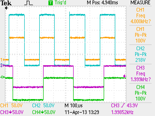
As the measurements in Figure 4 show, the options offered by the system make it possible to generate complex waveform patterns. To generate these signals the following parameters were varied:
amplitude,
frequency
and phase.
At low frequencies (\(\leq10~\textrm{kHz}\)) the output signals reach the full amplitude of \(400~\textrm{V}_{peak-peak}\). However, at higher frequencies the amplitude starts to drop due to thermal overload of the used linear regulator. Apart from this problem all major functions were verified and are functional.
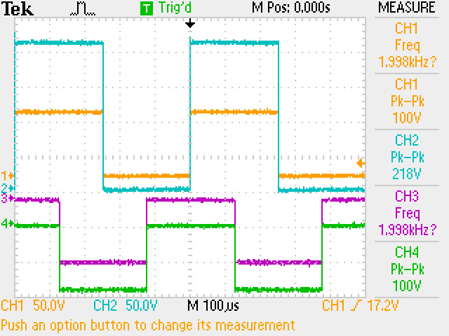
Measurements: basic signals.
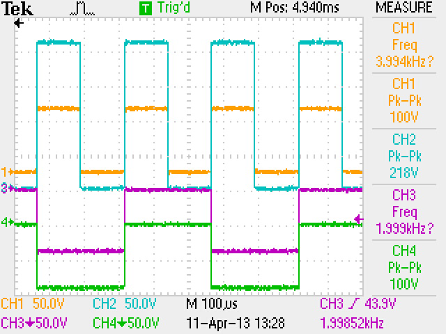
Measurements: signals of different frequencies.
Measurements: arbitrary phase shift between channels
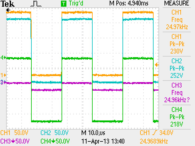
Measurements: high frequency signals.
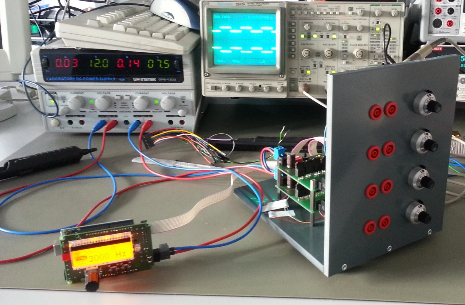
The completed circuit.
It was shown with the first two board revisions, that the chosen system design is up to the given task. All things considered, the required specifications could be satisfied.
But, as mentioned in Measurements, some problems with the circuit still remain:
The output amplitude drops at high switching frequencies. This problem is somewhat difficult to solve, as the current used by the H-bridge can not be reduced drastically because of switching losses.
Communication between the user interface board and the H-bridge boards is unstable at high switching frequencies. This can be solved with error correction in software and better PCB layout.
The overall efficiency of the circuit could be improved by using separate step-up converters for each channel.
To be able to change all parameters via the PC interface the output amplitude needs to be programmable from the micro-controller.
Implementing and verifying these changes will take at least one additional board revision.